
Microresistivity method
Precisely determine copper thickness on PCBs.
The microresistivity method is suitable for measuring the thickness of electrically conductive layers on insulating substrates according to ISO 14571. It is often used to check copper coatings on PCBs and multilayer PCBs. The advantage of the method is that other layers or interlayers in the PCBs have no influence on the measuring, so that the thickness can be determined precisely even with thin layers.
This is how the microresistivity method works.
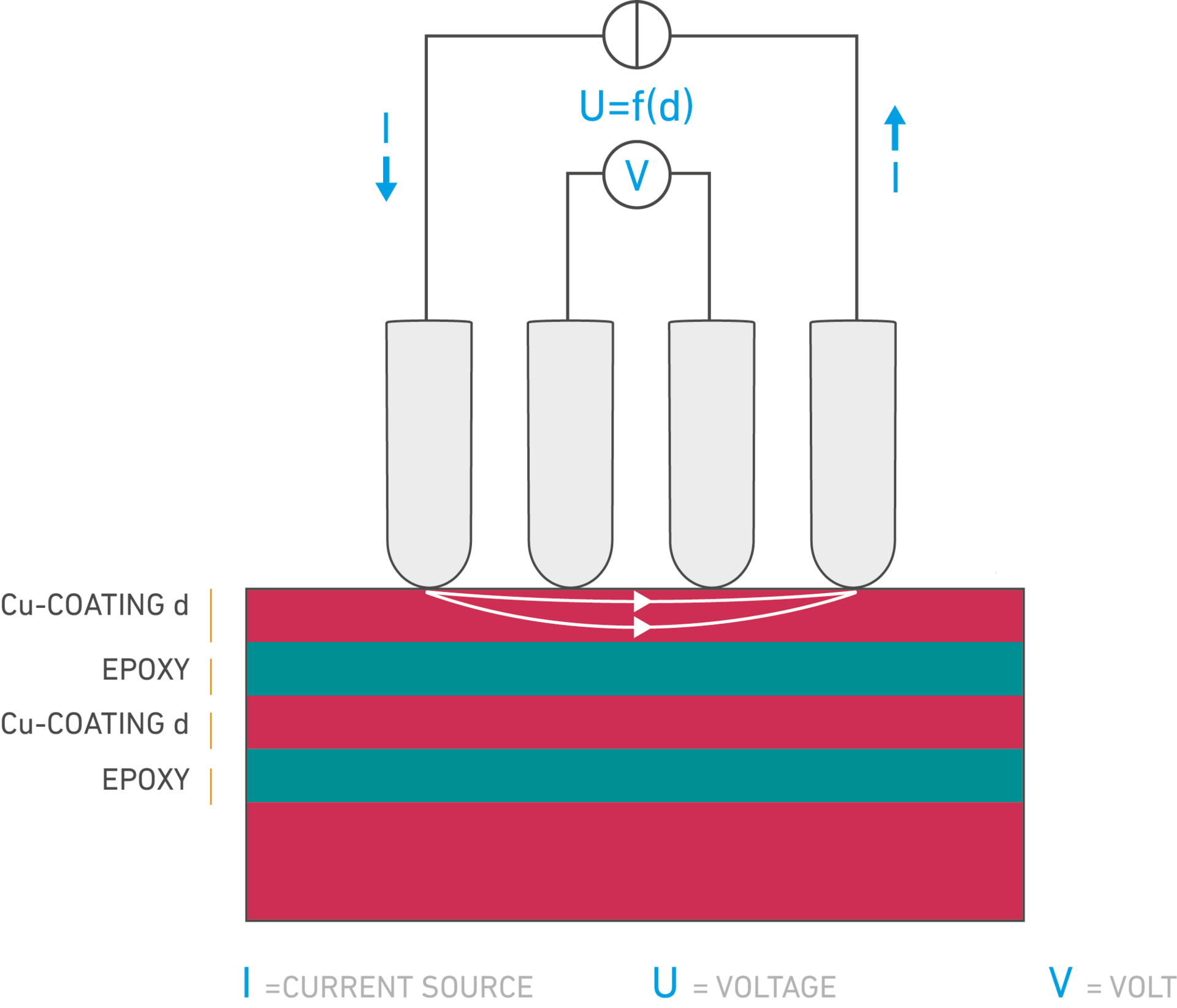
This method uses probes with four needles arranged in a row on the underside of the probe. When the probe is applied to the surface, current flows between the two outer needles. The coating acts as an electrical resistance across which a drop in voltage is measured with the two inner needles. The drop in voltage and thus the resistance increase as the coating thickness decreases, and vice versa.
Where is this process used?
- Control of copper coatings on PCBs and multilayer PCBs
What factors can influence the measurement?
All electromagnetic measuring methods are comparative. This means that the measured signal is compared with a characteristic curve stored in the device. To ensure that the result is correct, the characteristic curve must be adapted to the current conditions. This is done by calibrating the measuring device for coating thickness measurement.
The right calibration makes the difference
Factors that can strongly influence measuring the coating thickness are mainly: the specific resistivity of the copper layer and indirectly the temperature, the size of the measuring surface or conducting path and additional layers on the copper.
Specific resistivity and temperature
In addition to the coating thickness, the specific resistivity of the copper also influences the drop in voltage between the measuring needles. The resistance can differ depending on the alloy and processing of the metal. In addition, it varies at different temperatures. This may make temperature compensation or calibration under the measurement conditions necessary.
The size of the measuring surface
For narrow measuring surfaces, e.g. conductive paths, the currents run differently than for wide objects. This deviation from the theoretical currents leads to systematic errors in the coating thickness measurement. Therefore, there are probe-specific specifications for the minimum size of the sample or the minimum distance to the edge of the sample.
Additional layers
If there are other layers on the copper, such as tin, their layer thickness is measured by the probe in proportion to the copper thickness. How large the measurement error is depends on the ratio of the specific electrical conductivity of copper and the coating material.
Important
To counteract erroneous measurement results, the following influences must also be taken into account:
- Indentation errors with particularly soft coatings (such as phosphate coatings).
- Scatter increases due to wear of the probe pole; we recommend carrying out regular checks
Which standard is applied here?
Micro resistance method according to ISO 14571
Discover our measuring devices.